Zener Diode- Working, Construction, V I characteristic,Symbol and Application
Zener Diode is a special type of diode that can conduct in forward as well as in reverse bias mode. This special diode is named after American physicist Dr. Clarence Melvin Zener.
We will discuss working principles that underscore its distinctive behavior— specifically, construction, Zener effect, and avalanche breakdown.
The Symbol of a Zener Diode
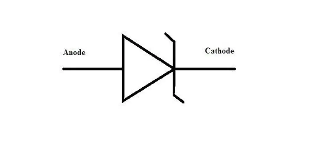
In electrical circuit diagrams and schematics, different components are represented by distinct symbols. For a Zener diode, its symbol is similar to that of a regular diode but with some modifications. It is depicted as a regular diode symbol, which looks like an arrowhead pointing towards a vertical line, but with an additional two lines at an angle in the tail of the symbol. These two lines are the enhancements over the regular diode symbol and indicate that the device is a Zener diode and can conduct in the reverse direction when a particular reverse voltage is reached.

Zener Diode Construction
The Zener diode, named after its inventor Clarence Zener, is a unique kind of diode. The primary structural component is a P-N junction (a key feature of all diodes) formed by doping a semiconductor material, such as silicon or germanium, with both P-type and N-type doping agents. This P-N junction is sandwiched between two metallic electrodes that serve as the leads for the device.
In terms of Zener diode construction, the difference between a standard diode and this diode lies in the level of doping. It is highly doped, resulting in a thin depletion layer compared to regular diodes. This thin depletion layer allows the Zener diode to have a lower breakdown voltage and function effectively in the reverse-bias mode.
Working Principle of Zener Diode
A Zener diode reveals its true characteristics and becomes distinctive when it is reverse-biased. As voltage is increased in the reverse direction, a certain threshold—called the Zener voltage or breakdown voltage—is reached, causing a large flow of current. This characteristic is due to two specific phenomena: the Zener effect and avalanche breakdown.
The Zener effect is a quantum mechanical effect that becomes dominant at voltages below 5V, whereby the high electric field enables the tunneling of electrons from the valence band to the conduction band, leading to a significant increase in current.
On the other hand, the avalanche breakdown is a phenomenon that takes over at voltages above 5V. It involves the acceleration of carriers to energies sufficient to free electron-hole pairs via collisions, dramatically increasing the current.
Regardless of the increase in current, the voltage across this diode remains steady at the Zener voltage, making the Zener diode useful as a voltage regulator.
The Zener voltage is dependent on temperature, with the Zener effect exhibiting a negative temperature coefficient and the avalanche breakdown showing a positive temperature coefficient. However, at a specific point called the “knee” (~5V), both effects co-exist and the overall temperature coefficient becomes nearly zero, which is a desirable trait for a voltage reference.
V-I Characteristic Curve of a Zener Diode
When examining the electrical characteristics, two primary features are considered: the zener voltage and the breakdown voltage.
The Zener voltage (Vz) is the specific voltage at which the diode begins to conduct in the reverse direction, and it is a predetermined value based on the level of doping in the P-N junction. This voltage can range from less than a volt to hundreds of volts based on the diode’s construction.
Another important feature of this diode is its current-voltage (I-V) characteristics. When forward biased, it will behave just like a regular diode. However, when reverse biased and the applied voltage reaches the Zener voltage, the diode enters the breakdown region and starts to conduct, allowing current to flow in the reverse direction.
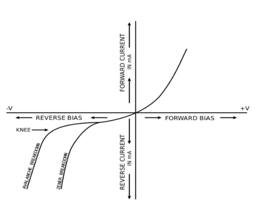
The VI characteristic curve of a Zener diode, also known as a Voltage-Current (VI) graph, defines its behavior under different operating conditions. This curve is divided into three primary zones: The forward bias region, the breakdown region, and the Zener region.
- Forward Bias Region: This is the region where the diode behaves like a typical P-N junction diode, allowing current to flow from the P-side (anode) to the N-side (cathode). In this region, the voltage increases linearly with the current.
- Breakdown Region: This region comes into play when the reverse bias voltage is increased beyond a critical point. The electric field across the depletion region becomes significant, leading to a rapid increase in current — a phenomenon known as ‘Zener Breakdown.’
- Zener Region: This is the region of operation unique to Zener diodes. In this region, even if the reverse bias voltage changes, the zener current remains relatively constant. This gives the zener diode its primary feature: Voltage regulation.
Understanding the Applications of Zener Diodes
Zener diodes, renowned for their ability to function uniquely under reverse bias conditions, are instrumental in numerous electrical applications, predominantly in the realm of voltage and power regulation.
- Voltage Regulation: Owing to their capacity to maintain a steady voltage across their terminals, regardless of current fluctuations, it is often employed in voltage regulator circuits, enabling a steady output voltage.
- Clipping and Clamping Circuits: These diodes find application in wave shaping circuits, with their ability to clip and eliminate signal voltages above or below specified levels.
- Voltage Stabilizers: Zener diodes are also used as voltage stabilizers in power supply circuits, safeguarding other electronic components from potential voltage surges.
- Waveform Generator: Leveraging the diode’s ability to swiftly switch between its low and high resistance states, they are also used in waveform generators to produce square, sine, or sawtooth waves as necessary.
- Switching Operations: it is instrumental in switching operations due to their consistent breakdown property under certain applied voltages.
In terms of device application, Zener diodes are found in numerous types of equipment and gadgets. For instance, they can be found in computers, cell phones, and televisions, acting both as voltage regulators and protection devices against voltage transients. They are widely used in power supply circuits to maintain a constant output voltage, regardless of input voltage fluctuations or changes in load conditions.